Trends
Transmission electron microscope market to reach USD 3.92B by 2030
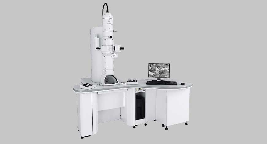
The report titled “Transmission electron microscope market by mode (Bright field, dark field), type (Aberration corrected TEM, Cryo-TEM, Environmental/In-situ TEM), product type, application, end users – Global Forecast 2024-2030” is now available on 360iResearch.com’s offering, presents an analysis indicating that the market projected to grow from a size of $2.05 billion in 2023 to reach $3.92 billion by 2030, at a CAGR of 9.71% over the forecast period.
“The rising importance of transmission electron microscopes in global research and development”
Transmission electron microscopy (TEM) is a pivotal analytical tool across various scientific disciplines, including nanotechnology, materials science, and biology. This advanced technology operates by channeling a high-energy beam of electrons through ultra-thin samples, rendering images that unveil structures at the atomic level. The increasing investments in research and development, coupled with the growing demand for intricate analysis in sectors such as electronics, semiconductors, and healthcare, have significantly amplified the need for TEM. Challenges include high costs, the necessity for specialized training, and complex sample preparation. Advancements are underway, including integrating AI and ML to address these hurdles. Regionally, the Americas, particularly the U.S. and Canada, are at the forefront of TEM adoption, owing to their robust investment in cutting-edge research fields. The APAC region, led by China, Japan, and India, is making swift advances, supported by governmental research funding and a keen focus on innovation. Europe’s strong R&D ecosystem, supported by governmental and EU funding, further complements the global outreach of TEM technology. The role of TEM in nanoworld is increasingly indispensable, highlighting its significance in propelling scientific and technological advancements globally.
“Revolutionizing semiconductor production with advanced imaging; the critical role of transmission electron microscopy”
In the rapidly advancing world of semiconductor manufacturing, the advent of transmission electron microscopy (TEM) marks a transformative step in producing and inspecting semiconductor devices. As the industry moves toward creating devices with finer details on the nanometer scale, the unparalleled resolution of TEM emerges as a vital tool. This advanced imaging technique provides an in-depth analysis of semiconductor materials, revealing critical insights into their structure and composition at an atomic level. TEM is essential in refining the manufacturing process, ensuring devices are high-performing and reliable by precisely identifying minuscule defects and material inconsistencies. Its ability to visualize the smallest details of device architecture assists in inspecting each manufacturing stage, preventing potential structural failures. The integration of TEM into the semiconductor manufacturing process highlights a commitment to excellence, paving the way for innovations that meet the growing demands for more powerful and efficient electronic devices. Through its contribution to material science and fabrication, TEM ensures the industry’s stride toward miniaturization and complexity in semiconductor devices remains steady and informed.
“The power of dark field TEM in unveiling microscopic defects”
Bright-field transmission electron microscopy (TEM) stands out for its ability to produce high-contrast images that reveal the intricate structures and dimensions of materials at the nano level, making it an indispensable tool for understanding the morphology of biological specimens, thin films, and nanoparticles. However, when investigating the hidden internal structures and defects of crystalline materials, Dark Field TEM emerges as a superior technique. Dark field TEM can visualize minute structural defects and dislocations that often go unnoticed, offering invaluable insights for materials science and engineering professionals. This method provides a detailed view of the material’s inner architecture, making it a go-to choice for those looking to delve deeper into the complexities of crystal structures and nanoparticles, contributing significantly to future advancements. 360iResearch


